The Scanning Tunneling Microscope (STM) gained instant international fame both in the scientific community as well as in mainstream culture by revealing images of atomic structure in real space for the first time. Since its invention by Binnig and Rohrer at the IBM laboratories in 1981, the STM has been a core tool of nanoscience. With STM, researchers have the ability to locally probe electronic states of the surfaces of conducting and semiconducting materials with extremely high energy resolution. It is also renowned for the ability to build and manipulate nanostructures one atom or molecule at a time. The main techniques we are currently using are imaging mode STM, scanning tunneling spectroscopy (STS), and quasiparticle interference (QPI).
STM Imaging
At the foundation of the STM is the quantum mechanical tunneling effect, whereby particles, in this case electrons, travel across a classically forbidden barrier. Its most basic and important properties can be easily derived from the direct application of the Schrodinger equation onto a plane wave traveling through a square potential. In STM, a metal tip is brought very close to the surface of a sample (on the order of angstroms), such that the wave functions of the tip and the sample overlap. If the wave function of the tip is assumed to remain constant throughout a scan, than the change in the signal will be due to the variations of the surface, as shown in the classic work of Tersoff and Hamman:
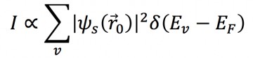
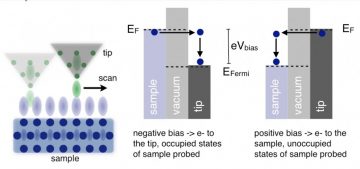
STM gives spatially resolved information of the electronic wave functions at the surface at a given potential, often termed the local density of states (LDOS). The current signal decays exponentially with sample‐tip distance, which results in extremely high z resolution. In scanning mode a bias is typically applied to the sample; if this bias is positive, electrons will flow to the sample giving information about unoccupied states of the surface, if the bias is negative, electrons will flow to the tip, giving information about the occupied states.
In imaging mode, a feedback loop typically maintains a constant current by varying the tip height above the sample, which is recorded as a function of position to create a constant current topographic map. It is important to note that STM does not measure true topographic features of the surface, even though it is recording the change in height of the tip, rather it reflects the electronic environment. The voltages can be manipulated to visually image the electronic features of a surface, including the molecular orbitals, surfaces states, charge distribution, and many other electronic features.
Scanning Tunneling Spectroscopy (STS)
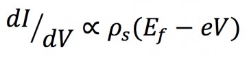
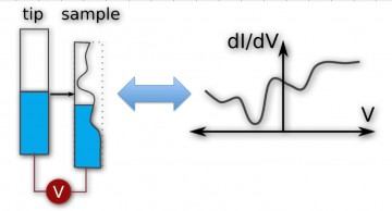
The second power of the STM is the ability to perform local spectroscopy. STS is able to probe the density of states (DOS) as a function of energy, i.e. the number of electrons at a given energy. The main method used here is the measurement of change in current as a function of applied voltage with the tip held at a constant height. Since dI/dV is proportional to the density of states of the sample, p, the derivative of this curve corresponds to the LDOS, see equation below, where Ef and V are the Fermi energy and bias voltage respectively. The derivative can be taken numerically, or acquired with the use of a lock-in amplifier.
Quasiparticle Interference (QPI)
STM has become a key tool for the investigation of superconducting materials by combining the high spectroscopic energy resolution possible in tunneling measurements with the high spatial resolution a scanning probe technique can provide. This reveals information regarding the quasi-particle excitations, the local density of states variations arising from dopants, and the influence and electronic structure of defects. Further, dense spectroscopic grids can be used to obtain both real-space and k-space information arising from scattering processes. These “4d” spectroscopic grids benefit from extremely low noise levels as this allows faster individual spectra enabling larger areas and denser point meshes.