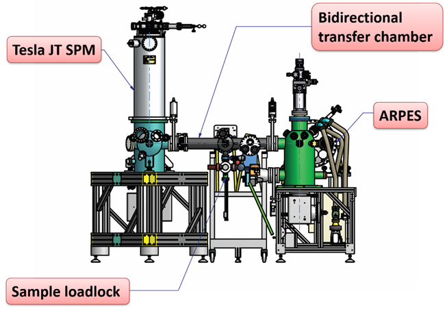
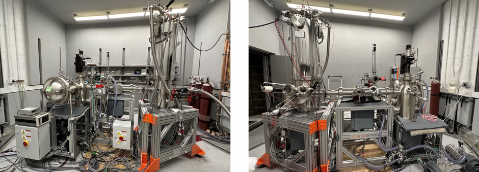
This integrated system is the newest addition to the LAIR fleet (commissioned in 2019) at 61 Brimacombe. Its Joule-Thomson (JT) STM/AFM operates at 1 K with 170 hr long LHe holding time, enabling undisturbed long measurements such as quasiparticle interference up to a week with better resolution. It is also equipped with a dry superconducting split-pair 1D magnet for a vertical magnetic field up to 3 T. A standard STM tip and a Qplus AFM tip can be used in this JT system, making it capable of spin-polarized STM and magnetic force microscopy combined with the magnetic field.
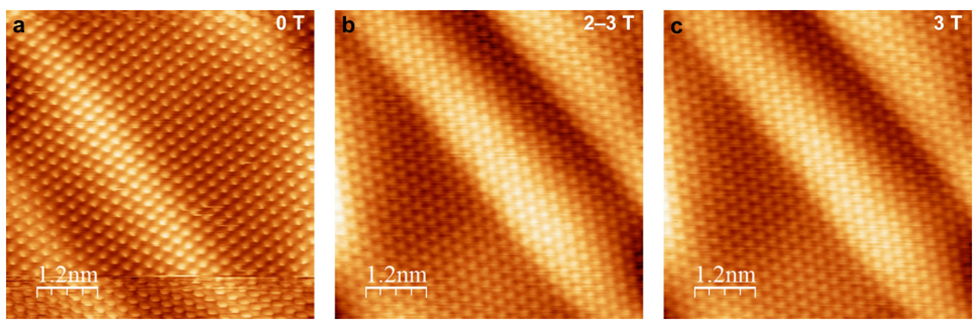
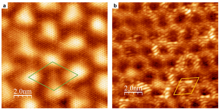
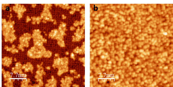
The JT STM/AFM is connected to the ARPES system via a bidirectional transfer chamber, as shown in Figs. 1 and 2. JT STM/AFM provides a range of tools for acquiring local atomic-scale views of the structure and electronic states of materials. ARPES provides a complementary view of the electrons delocalized across the surface but with a high resolution of their electronic structure in momentum space. This integrated JT STM/AFM-ARPES system gives us the advantage of characterizing surface electronic properties in real and k-space on the very same sample. Our ARPES is optimized for quick high-resolution photoemission spectroscopy measurements and equipped with the cooling and heating sample stage, ranging from -130 °C to 830 °C. The main research interests z of Tesla are studying quantum materials such as graphene, high TC superconductors, and topological semimetals. Some representative images taken on these samples are shown in Figs. 3-5.
[1] Amy Qu, Atomic modification of graphene on silicon carbide: adsorption and intercalation, http://hdl.handle.net/2429/79480